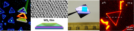
The rise of two-dimensional (2D) materials has opened up possibilities for exploring new physical phenomena that motivate the synthesis of more complex low dimensional systems. In this plenary talk, we will discuss doping routes that allow the tunability of electronic properties in 2D semiconducting transition metal dichacogenides (TMDs). Zero dimensional (0D) defects such as vacancies and substitutional dopants within tungsten disulfide (WS2) monolayers, will be discussed. In particular, molybdenum doping of WS2 monolayers can lead to one dimensional metallic atomic chains of Mo embedded within the WS2 lattice, as observed by high–resolution scanning transmission electron microscopy (HR-STEM) studies. These 2D systems also exhibit different band gaps within the same monocrystalline flake. Regarding TMD doping with CH units, a novel radio-frequency plasma assisted (RF-PA) approach will be introduced. Electron microscopy studies confirmed the presence of CH units within the WS2 lattice of plasma treated islands, and DFT calculations confirm the stability of these CH species in sulfur mono-vacancies. Furthermore, field effect transistors fabricated using these CH-doped WS2 exhibit an ambipolar behavior, instead of the n-type transport showed by pristine WS2. Finally, the photoluminescence (PL) emission (at 77K) of defective TMD monolayers will be presented. In particular, sulfur mono-vacancies concentrated along the edges of triangular WS2 monocrystals led to the appearance of bound excitons located 300 meV below the neutral (A) exciton. DFT calculations reveal that sulfur monovacancies introduce midgap states exactly 300 meV below the edge of the conduction band. Finally, challenges and new directions in defect engineering of 2D materials will be envisaged.
Figure: Photoluminescence enhancement in WS2; growth of large area atomically thin WS2; bound defect exciton detected at 77K in defective WS2.