Applied Physical Chemistry, Heidelberg University, 69120 Heidelberg, Germany
Self-assembled monolayers (SAMs) are 2D polycrystalline films of semi-rigid molecules that are chemically anchored to a suitable substrate. Blocking the substrate off the ambient, a SAM gives the surface a new physical and chemical identity, which can be precisely adjusted by the selection of the SAM constituents. These can be flexibly designed by a suitable combination of the individual building blocks, which are a headgroup that makes the anchoring to the substrate, a tail group that is exposed to ambience, and a spacer that separates the head and tail groups. The flexibility of the SAM design and the possibility to prepare these films on almost any substrate result in a variety of applications, such as e.g. tailoring surface properties (wetting, adhesion, lubrication, corrosion, and biocompatibility), sensor fabrication, molecular and organic electronics (injection barrier and growth mode), and conventional and chemical lithography. In most cases, these applications rely on a specific architecture of SAM constituents and SAM as a whole as well as on precise knowledge of the SAM properties. In the overview talk, I will describe the basic properties and architecture of SAMs, address the current state of understanding of the molecular self-assembly, and give representative examples for design of application-relevant SAMs on noble metal and semiconductor substrates. The emphasis will be put on tailoring molecular organisation to achieve specific structural organization of the fabricated films as well as to create a definite chemical identity of the functionalized substrate. This is a prerequisite for well-defined chemical and physical properties of the modified surface. Several examples of application-related molecular design will be given, viz., in the areas of molecular electronics, control of electronic coupling at the interfaces, nanofabrication, chemical lithography, and biofunctionalization.
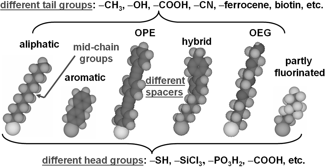
Typical molecular precursors of self-assembled monolayers. OPE and OEG are abbreviations for oligo(phenyleneethynylene) and oligo(ethylene glycol), respectively.
Summary of academic career
Michael Zharnikov has received a Master degree (with honor) in Solid State Physics from the Moscow Engineer-Physical Institute in 1981. From 1981 to 1991 he worked in Kurchatov Atomic Energy Institute in Moscow, where he received a PhD degree in Experimental Physics in 1989. In 1991 he moved to Germany. After 2 post-doctoral stints with Prof. Dietrich Menzel at the Technical University Munich (1991-1994) and Prof. Jürgen Kirschner at Max-Planck Institute für Mikrostrukturphysik in Halle/Saale (1994-1996), Zharnikov joined the Faculty of Chemistry and Geosciences at the Heidelberg University first as Senior Scientist (group of Prof. Michael Grunze) and later, after habilitation, as Privat-Dozent (2001) and Prof. apl. (2008). Zharnikov published 287 peer-reviewed journal articles and book chapters (H=46, ca. 8100 citations), obtained 2 patens, and delivered about 140 lectures, including 55 invited talks at national and international conferences. His group at Heidelberg University is actively involved in research related to the fabrication of functional organic surfaces, interfacial engineering, biointerfaces, molecular sensors, soft matter nanofabrication, e-beam and UV lithography, molecular and organic electronics, design of novel materials, molecular structure of liquids, and advanced X-ray spectroscopy. His activities involve a frequent use of synchrotron radiation facilities over the world, including BESSY II in Berlin, Max IV in Lund, and ALS in Berkeley. Zharnikov is a member of the Editorial Boards of J. Electron Spectrosc. Relat. Phenom. and J. Vac. Sci. Technol.